 |
VOOZH | about |
|
VOOZH | about |
Because of its low power consumption and high input impedance, MOSFET is frequently utilized in electronic circuits. MOSFETs are more efficient than Bipolar Junction Transistors (BJTs) since they do not need a lot of input current. Because the gate and channel are isolated in MOSFETs, there is very little gate current and less power loss.
Biasing is the process of giving the MOSFET the proper DC voltages and currents to function in the required region, usually the saturation region for amplifier applications. The circuit will operate steadily and behave as intended with proper biasing.
Typical methods for biasing MOSFETs include:
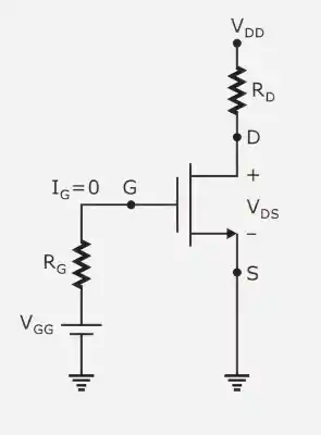
The gate voltage in the gate bias circuit is fixed by an external voltage source. There is no voltage drop across the gate resistor in a MOSFET since the gate current is zero (). As a result, the applied bias voltage equals the gate voltage.
Given that the source is typically grounded:
KVL application in the drain circuit:
In order to properly bias in the saturation region:
The MOSFET can be biased in the desired region by choosing the right gate voltage and drain resistance settings.
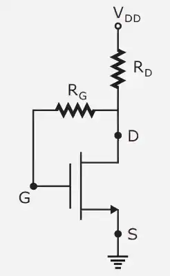
A separate gate supply is not required thanks to the drain-to-gate bias circuit. Here, automatic biasing is achieved by connecting the gate to the drain via a resistor.
There is no voltage drop across the gate resistor since . Hence:
Therefore:
KVL application in the circuit:
In this setup:
The MOSFET functioning is naturally stabilized by this biasing technique, which usually maintains it in the saturation area.
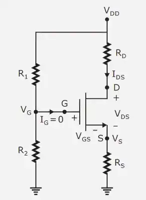
The gate voltage in this circuit is set using a voltage divider network (and ), which improves control and stability over earlier techniques.
Given that , the gate voltage is determined by:
Source voltage:
Thus:
KVL application in the drain circuit:
In order to function properly in the saturation region:
This technique is frequently utilized in real-world circuits and offers good bias stability.
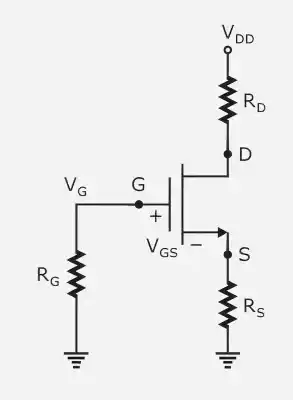
The source resistor in the self-bias circuit is used to bias the gate, which is coupled to ground via a resistor.
Given that :
KVL application from gate to source:
From the relationship mentioned above:
This demonstrates that in this configuration, is negative.