
Solid-state drives (SSDs) have significantly evolved data storage, moving away from the mechanical design of Hard Disk Drives (HDDs) towards a more efficient, semiconductor-based approach. SSDs use flash memory, which provides faster data access, increased durability, and greater energy efficiency. This article aims to demystify the complex technology behind SSDs, focusing on their components and how they manage data storage and retrieval.
Structure of an SSD and its components
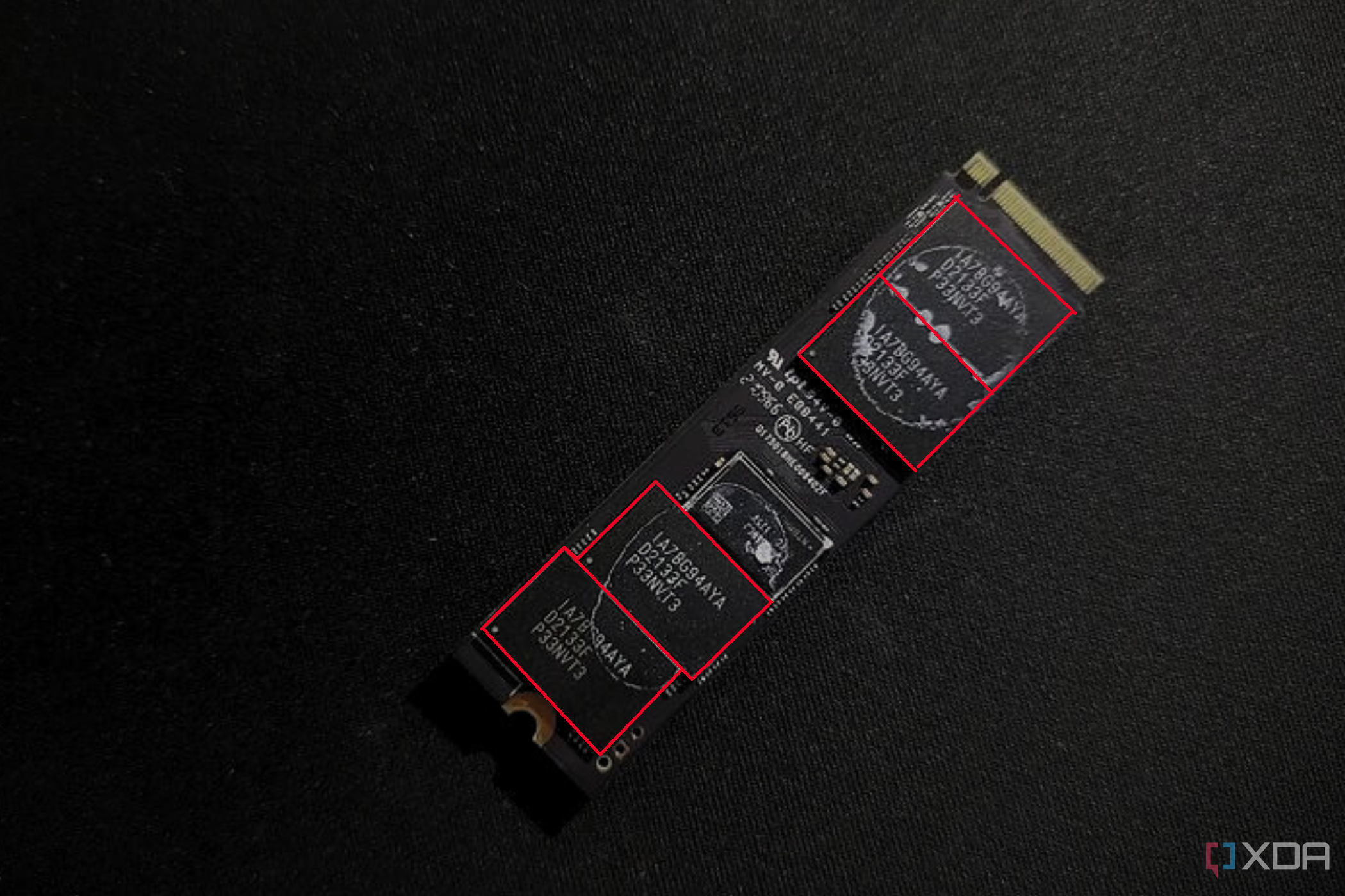
👁 Image showing the NAND Flash chips on a MSI Spatium M480 on a black background
NAND Flash
At the heart of an SSD lies its integrated circuit, a complex assembly of electronic circuits intricately embedded within a silicon semiconductor cell. This integration is key to the SSD's ability to store vast data in a compact form factor.
SSDs rely on flash memory for data storage, characterized by its non-volatile nature. This means that data is retained even when the SSD is not powered. The structure of this flash memory in SSDs is based on NAND technology, where data is organized into a grid of blocks, each comprising an array of pages or sectors. These are the smallest units for data storage and access within the SSD. The efficient organization and accessibility of these blocks and pages are what enable SSDs to offer speed and performance, significantly outstripping the capabilities of traditional hard disk drives.
The fundamental mechanism for data storage in SSDs is provided by floating gate transistors (FGTs) within the NAND flash memory. These transistors have the unique ability to hold an electrical charge, which is used to represent binary data. The microscopic transistors and capacitors in SSDs can be charged to represent "1" or discharged to represent "0" by applying different voltages, thereby storing or releasing a tiny amount of electric charge in a controlled manner. This process of manipulating electrical charges at a microscopic level allows SSDs to achieve exceptionally fast data access speeds, far surpassing the performance of HDDs.
SSD controller
The SSD controller, a sophisticated microprocessor that acts like a CPU, is central to the drive's functionality and performance. It manages a suite of complex algorithms, each designed to optimize data handling and storage longevity. One key algorithm is wear leveling, which intelligently distributes data written across the NAND flash memory. This strategy mitigates the uneven wear of memory cells so that each cell has the same approximate longevity. By ensuring that no single cell is overused, wear leveling significantly extends the SSD's overall lifespan. Error Correction Code (ECC) is another critical algorithm. As data integrity has to be ensured in the continuous coding and decoding, ECC algorithms work relentlessly to detect and correct bits of data that may have been altered or corrupted during storage or transmission.
This process involves generating additional data bits during writing, which are used for comparison and error correction during reading. The sophistication of ECC algorithms directly influences the reliability and accuracy of data retrieval in SSDs. Additionally, the controller executes bad block mapping, identifying and isolating damaged or worn-out cells (bad blocks). It then remaps data storage to healthy cells, ensuring data integrity and consistent performance. This proactive management prevents data loss and maintains the drive's efficiency.
DRAM Cache
Many SSDs include a DRAM cache, which serves as a fast-access memory pool for storing temporary data and mapping tables (the directory to the location of the entire data). This significantly speeds up data retrieval processes, reducing the time it takes for the SSD to locate and access data. The DRAM cache is a key component in enhancing the overall responsiveness and efficiency of an SSD.
How does data storage work in SSDs?
Writing data
Writing data to an SSD is a precise and complex process. It begins with data encoding, which converts information into a format suitable for storage using the Error-Correcting Code (ECC). Data is then written in 'pages,' which is the smallest unit of data for writing. However, erasing data requires clearing entire 'blocks,' which are groups of pages. This characteristic necessitates the Program/Erase cycle, where a full block is erased and rewritten, even for small data changes. Wear leveling (handled by the controller) comes into play here, as the controller spreads out these cycles across the memory cells to prevent any single cell from being overused and worn out prematurely.
Reading data
Reading data from an SSD involves the controller locating the correct block and page. It then reads the stored charge from the memory cells, interpreting this as binary data. During this process, ECC algorithms detect and correct errors, ensuring the accuracy and integrity of the retrieved data.
NAND flash types and their impacts
1. SLC (Single-Level Cell) NAND:
SLC NAND stores one bit per cell, providing the highest speed and endurance among NAND types. This makes it ideal for high-performance applications but comes at a higher cost due to its lower storage density and more complex manufacturing process.
2. MLC (Multi-Level Cell) NAND:
MLC NAND stores two bits per cell, striking a balance between cost and performance. It is more cost-effective than SLC due to higher data density but has moderately lower speed and endurance. MLC is commonly used in consumer-grade SSDs and enterprise applications where a balance of performance and cost is necessary. The term MLC can apply to any cell that stores more than one bit per cell, but it's more commonly used for two-bit cells.
3. TLC (Triple-Level Cell) NAND:
TLC NAND, storing three bits per cell, offers even greater cost efficiency by increasing the storage density. However, this comes at the expense of reduced speed and lifespan compared to MLC. TLC NAND is often used in budget-friendly SSDs where large storage capacity is prioritized over top-tier performance.
4. QLC (Quad-Level Cell) NAND:
QLC NAND, with four bits stored per cell, provides the highest density for storage, translating to the largest capacity at the lowest cost. However, this advantage is offset by the lowest endurance and slower performance relative to the other types. QLC is suitable for applications where storage capacity is more critical than speed or longevity, like in some consumer storage devices.
Complications with SSDs
Write amplification is a phenomenon in SSDs where the actual amount of data written exceeds the intended data. This occurs during the Program/Erase cycle and can adversely affect the SSD's lifespan. Additionally, SSDs employ a process called garbage collection, which involves rearranging and consolidating data for efficient memory block usage. While essential for maintaining optimal storage efficiency, garbage collection can temporarily hinder SSD performance, particularly during heavy data-writing operations.
Over time, the repeated use of NAND cells in SSDs leads to data degradation, impacting performance and longevity. To counteract this, techniques such as over-provisioning are used, where extra storage capacity is reserved to replace worn-out cells. Furthermore, the TRIM command plays a vital role by enabling the operating system to notify the SSD of which data blocks are no longer in use, allowing for more efficient data management and helping to preserve the health and efficiency of the SSD over its lifespan.