 |
VOOZH | about |
|
VOOZH | about |
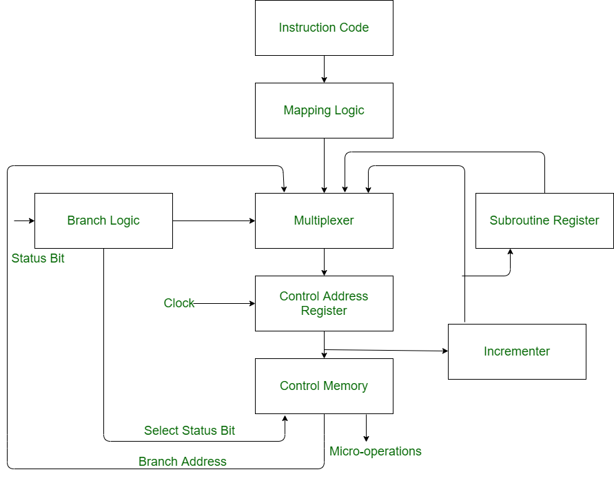
The address is used by a microprogram sequencer to decide which microinstruction has to be performed next. Microprogram sequencing is the name of the total procedure. The addresses needed to step through a control store's microprogram are created by a sequencer, also known as a microsequencer.
The control unit's main job is to communicate with the computer's memory, input/output device, and ALU on how to respond to or carry out a set of instructions. Processing is not done within the Control unit itself. It only directs and manages the task. It serves as the computer's supervisor, regulating all operations including retrieving instructions from main memory and putting them to use.
Micro Instructions Sequencer is a combination of all hardware for selecting the next micro-instruction address. The micro-instruction in control memory contains a set of bits to initiate micro-operations in computer registers and other bits to specify the method by which the address is obtained.
A set of micro-instructions make up microprogramming. Three micro-operation phases are primarily present in each micro-instruction. F1, F2, F3, respectively. We also have the condition, branch, and address fields in addition to these three.
A 3X8 decoder decodes the F1, F2, and F3 fields because they are all 3 bits in size. We receive 8 outputs from the F1 micro-operation phase. One of these eight outputs is still unutilized.
Like the F1 procedure, the F2 operation produces a total of 7 outputs.
Only six operations can be carried out in the F3 micro-operation phase (one is left unfinished, and the other is saved for later use).
Therefore, we can complete 20 micro-operations in total (7+7+6).
Out of 20 operations, the diagram above shows 5 micro-operations.
The ALU is attached to F2 output number 3. It applies the AND operation to the contents of the data register and accumulator, then transfers the outcome to the accumulator. This is how it is written: ACAC AND DR
And we give the matching accumulator a clock pulse. The ability to load it onto the accumulator is enabled.
Output 1 of F1 adds data register and accumulator using an ALU, then sends the outcome to the accumulator.
The DRTAR operation, or transfer of the contents of the data register to the address register, is carried out by output 5 of F1. However, the data register's size is 16 bits, while the the rightmost significant 12 bits of the data register are moved to the address register since the address register only has a capacity of 12 bits.
Transferring the contents of the programme counter to the address register is what output 6 of F1 does.