 |
VOOZH | about |
|
VOOZH | about |
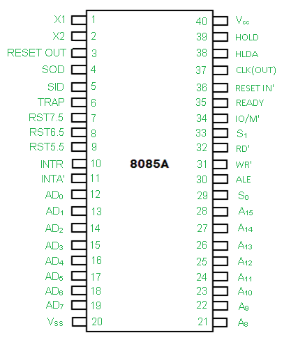
The 8085 microprocessor is a popular 8-bit microprocessor developed by Intel. It has 40 pins, each with a specific function for interfacing with memory, input/output devices, and other components.
Pin diagram of 8085 microprocessor is shown below:
Address Bus (A8 to A15): The address bus is unidirectional, i.e., bits flow in one direction from the microprocessor unit to the peripheral devices and uses the higher order address bus.
Address Data Bus (AD0 to AD7): These are bi-directional data pins used to transfer data between the microprocessor and memory or I/O devices. The microprocessor is an 8-bit processor, so it uses 8 data lines. These pins serve the dual purpose of transmitting lower order address and data byte. During 1st clock cycle, these pins act as lower half of address. In remaining clock cycles, these pins act as data bus.
ALE - It is an Address Latch Enable signal. It goes high during first T state of a machine cycle and enables the lower 8-bits of the address, if its value is 1 otherwise data bus is activated.
IO/M' - It is a status signal which determines whether the address is for input-output or memory. When it is high(1) the address on the address bus is for input-output devices. When it is low(0) the address on the address bus is for the memory.
SO, S1 - These are status signals. They distinguish the various types of operations such as halt, reading, instruction fetching or writing.
| IO/M' | S1 | S0 | Data Bus Status |
|---|---|---|---|
| 0 | 1 | 1 | Opcode fetch |
| 0 | 1 | 0 | Memory read |
| 0 | 0 | 1 | Memory write |
| 1 | 1 | 0 | I/O read |
| 1 | 0 | 1 | I/O write |
| 1 | 1 | 1 | Interrupt acknowledge |
| 0 | 0 | 0 | Halt |
RD' - It is a signal to control READ operation. When it is low the selected memory or input-output device is read.
WR' - It is a signal to control WRITE operation. When it goes low the data on the data bus is written into the selected memory or I/O location.
READY - It senses whether a peripheral is ready to transfer data or not. If READY is high(1) the peripheral is ready. If it is low(0) the microprocessor waits till it goes high. It is useful for interfacing low speed devices.
Vcc - +5v power supply
Vss - Ground Reference
XI, X2 - A crystal is connected at these two pins. The frequency is internally divided by two, therefore, to operate a system at 3MHZ the crystal should have frequency of 6MHZ.
CLK (OUT) - This signal can be used as the system clock for other devices.
4. Interrupts and Peripheral Initiated Signals:
The 8085 has five interrupt signals that can be used to interrupt a program execution.
(i) INTR
(ii) RST 7.5
(iii) RST 6.5
(iv) RST 5.5
(v) TRAP
The microprocessor acknowledges Interrupt Request by INTA' signal. In addition to Interrupts, there are three externally initiated signals namely RESET, HOLD and READY. To respond to HOLD request, it has one signal called HLDA.
RESET IN - When the signal on this pin is low(0), the program-counter is set to zero, the microprocessor unit is reset.
RESET OUT - This signal indicates that the MPU is being reset. The signal can be used to reset other devices.
HOLD - It indicates that another device is requesting the use of the address and data bus. Having received HOLD request the microprocessor relinquishes the use of the buses as soon as the current machine cycle is completed. Internal processing may continue. After the removal of the HOLD signal the processor regains the bus.
HLDA - It is a signal which indicates that the hold request has been received after the removal of a HOLD request, the HLDA goes low.
Serial transmission in 8085 is implemented by the two signals.
SID and SOD - SID is a data line for serial input whereas SOD is a data line for serial output.