 |
VOOZH | about |
|
VOOZH | about |
A P-N junction diode is a two-terminal semiconductor device formed by joining p-type and n-type semiconductors, creating a junction at their boundary.
To understand the formation of a p–n junction, consider a thin p-type silicon semiconductor sheet. If a small amount of pentavalent impurity (valency 5) is added to a portion of this sheet, that part of the p-type silicon is converted into n-type silicon. As a result, the same semiconductor crystal now contains both p-type and n-type regions. The boundary formed between these two regions is called the p–n junction.
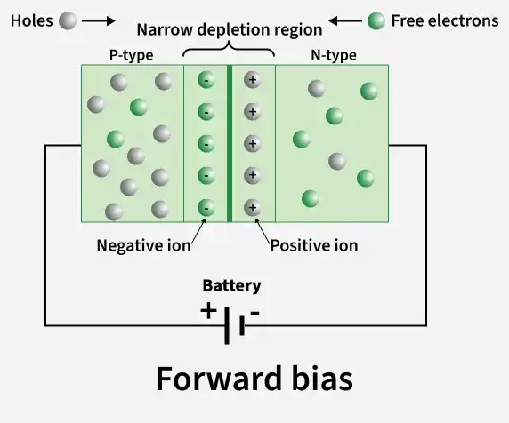
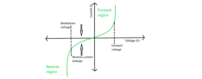
Forward bias is the condition in which a p–n junction diode is connected to an external voltage source such that the p-type region is connected to the positive terminal and the n-type region to the negative terminal of the battery. In this condition, the applied electric field opposes the junction's built-in potential barrier, reducing its strength. As a result, the depletion region becomes thinner, the junction resistance decreases, and current flows easily through the diode once the applied voltage exceeds the threshold value (about 0.7 V for silicon).
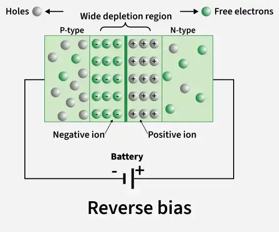
Reverse bias is the condition in which a p–n junction diode is connected to an external voltage source such that the n-type region is connected to the positive terminal and the p-type region to the negative terminal of the battery. In this arrangement, the applied electric field is in the same direction as the built-in electric field, which increases the potential barrier. As a result, the depletion region becomes wider, the junction resistance increases, and only a very small leakage current flows. If the reverse voltage is increased further, the depletion layer becomes even thicker and more resistive until breakdown occurs at a sufficiently high voltage.
The potential difference created by the electric field in the p-n junction is given by:
- E0= junction voltage at no bias
- VT = thermal voltage (≈ 26 mV at room temperature)
- ND = donor concentration
- NA = acceptor concentration
- ni = intrinsic carrier concentration
Question 1: A transistor has a current gain of 30. If the collector resistance is RC = 6 kΩ and the input resistance is Rin = 1 kΩ, calculate the voltage gain.
Solution: Resistance gain =
Voltage gain = Current gain × Resistance gain
Question 2: A P-N junction has ND = 5 × 1015 cm⁻³, NA = 2 × 1016 cm⁻³, and ni = 1.5 × 1010 cm⁻³.. Find the built-in potential E0 at room temperature (VT = 0.026 V).
Solution: The built-in potential of a P-N junction is given by,
Substitute the values
Question 3: A diode has a forward resistance of 500 Ω. If a voltage of 0.6 V is applied, calculate the forward current.
Solution: Using Ohm's law
Substitute the values
Question 4: A silicon diode is forward-biased with a voltage of 0.8 V. The diode has a saturation current IS = 10-12 A and thermal voltage VT = 0.026 V. Calculate the forward current. I using the diode equation
Solution: Substitute the given values
Question 1: A P-N junction diode has a forward voltage of 0.65 V. The diode has a resistance of 250 Ω in the forward direction. Calculate the current through the diode.
Question 2: A silicon diode is reverse-biased with 10 V. The saturation current Is = 5 × 10⁻¹³ A. Find the reverse current flowing through the diode.
Question 3: The donor concentration in the n-type region is ND = 1017 cm⁻³and the acceptor concentration in the p-type region is NA = 2 × 1016 cm⁻³.. If the intrinsic carrier concentration is ni = 1.5 × 1010 cm⁻³and VT = 0.026 V, calculate the built-in potential E₀..
Question 4: A diode has a saturation current IS = 2 × 10⁻¹² A and thermal voltage VT = 0.026 V. Calculate the forward current if the applied voltage is 0.75 V using the diode equation.
Question 5: A diode is forward biased with 0.7 V. If the diode’s forward resistance is 500 Ω and the saturation current IS = 10-12 A, estimate the total current through the diode, considering both the resistance and diode equation effect.