 |
VOOZH | about |
|
VOOZH | about |
A universal gate is such a gate that we can implement any Boolean function, no matter how complex, using a circuit that consists of only that particular universal gate. The NAND & NOR gates are the most commonly encountered universal gates in digital logic.
In this article, we will take a look at how to convert any circuit into a circuit that consists only of NAND gates. Since the NAND gate is a universal gate, we can convert any circuit into a circuit consisting only of NAND gates. We first start by showing how other gates(AND, OR, Inverter) can be implemented using only NAND gates, then we use this knowledge to discuss how to convert any circuit into only a NAND circuit.
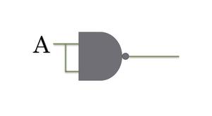
The NAND gate is a simple form of a Digital Logic gate which gives a False output if all the inputs are True. The device is an inverse of the AND gate. In Boolean algebra the NAND operation is represented as (AB)’. NAND gates are common in digital electronics since it is simple and can be used as a basis of most of the circuits. With gates NAND has one special feature which is that from them it is possible to construct any other function, it really works as a universal gate. This implies that, in principle, an entire digital circuit can be built using only NAND gates and this explains why they are very useful in circuit design.
Truth Table:
A | B | Output |
|---|---|---|
0 | 0 | 1 |
0 | 1 | 1 |
1 | 0 | 1 |
1 | 1 | 0 |
In this table it can be observed that the output is false only when both inputs A and B are true. For the output in all other cases, the value is true.
Given a circuit, our task is to implement a circuit that is equivalent to the given circuit and consists of only NAND gates.
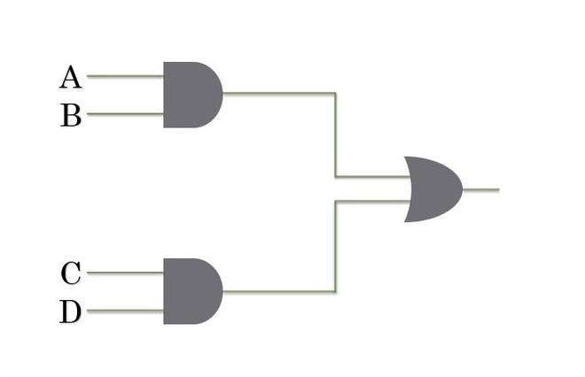
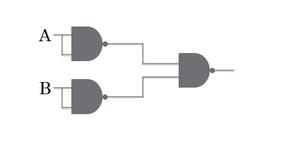
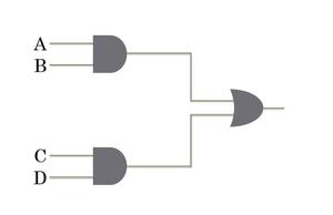
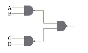
Example 1:
Given Circuit:
Same Boolean Function with NAND only Circuit
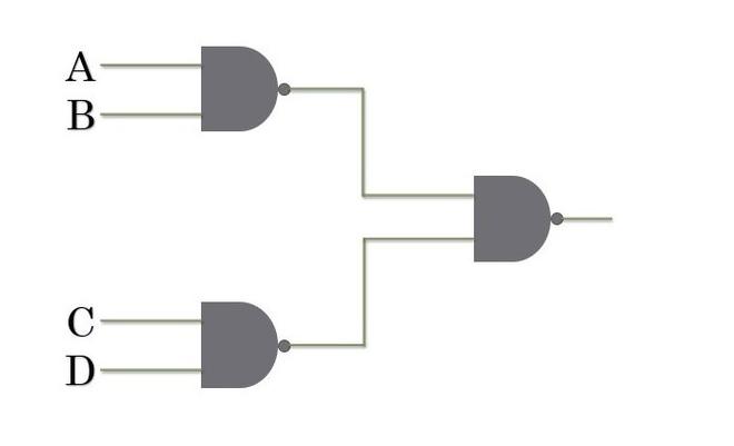
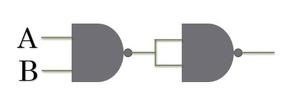
Example 2:
Given Circuit:
Same Boolean Function with NAND only gate circuit:
Before we get to how to convert any circuit to a NAND-only circuit, we will take a look at how to implement Complement, AND & OR operation using NAND gates. We also will need to take a look at how to implement NAND operation using OR gate.
This is quite straightforward, we wish to obtain AB but the NAND gate gives an output (AB)' so we complement the output of the NAND gate using another NAND gate to obtain ((AB)')' which is AB.
We first complement the inputs A and B. Then we perform the NAND operation on these complemented inputs. We get (A'B')'.
Using De-Morgan's law we can show that (A'B')' = A + B.
To implement NAND operation using OR gate, we first complement the inputs and then perform OR on the complemented inputs.
We get A' + B'.
A' + B' is equivalent to (AB)' which can be shown to be true by using De-Morgan's law.
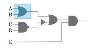
Consider the following circuit.
We have:
We have to somehow re-implement this circuit using only NAND gates.
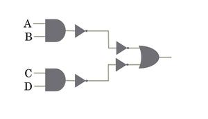
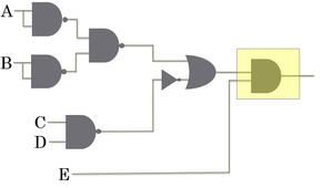
Suppose what happens if we insert two inverters between each AND gate and OR gate.
This circuit is completely equivalent to the original one as the output of each AND gate is being complemented twice before the signal reaches the OR gate. These inverters will play a key role in the process of conversion.
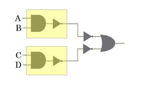
Now take a look at the highlighted areas.
The gates in each highlighted area can be easily combined into one NAND gate since it is basically just an AND gate followed by an inverter.
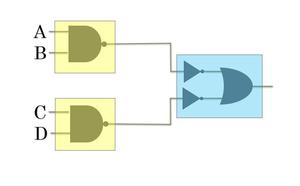
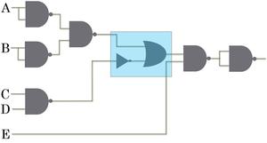
We get:
Now we only have to take care of the blue highlighted area. Recall the implementation of a NAND operation using OR & inverter gates we have covered above, the gates in the blue area implement a NAND operation. Therefore we can just replace all the gates in the blue area with a single NAND gate!
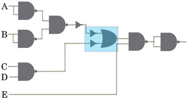
Our Final Result:
You can verify for yourself that this circuit implements the function AB + CD, same as that of the original circuit.
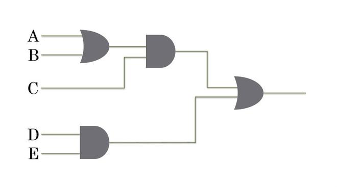
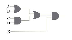
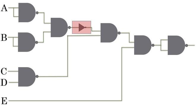
Another Example:
Original Circuit:
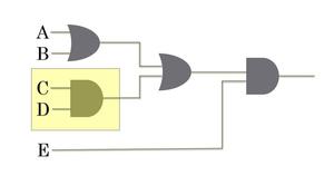
Method 1
First, we start by replacing the first AND gate(highlighted yellow) with a NAND gate. To do this we insert two inverters after this AND gate.
Remember that this circuit is the same as two complement operations resulting in the original signal. The AND gate and the inverter that follows it can be combined into a single NAND gate(see yellow highlighted area).
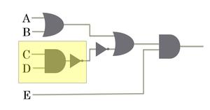
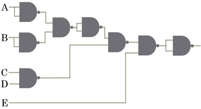
Next, we replace the OR gate in the blue highlighted area with NAND gates. We have seen how to implement OR operation using NAND gates, we put that knowledge to use now.
We then proceed to replace the last AND gate(highlighted yellow) with NAND gates. Just like we replaced the OR gate in the previous step, we replace the AND gate with its equivalent NAND gate circuit.
We now are left with an OR Gate and an Inverter Gate. A NAND gate can be implemented by an OR gate with complemented inputs. Here we have only one complemented input to the OR gate. To meet the condition that both the inputs are complemented, we insert two inverters between the highlighted OR gate and the preceding NAND gate.
We get:
Now both the inputs to the OR gate are complemented. The gates in the blue area represent a NAND operation so we can replace them with a NAND gate.
We are now only left with an Inverter. An Inverter gate is basically a one-input NAND gate. We make the necessary replacement and obtain our final circuit.
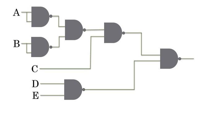
Our Final NAND gate-only circuit:
You can verify that this circuit implements : (A+B + CD)E
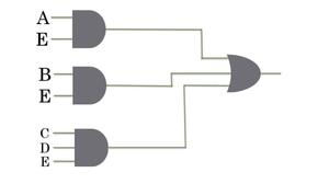
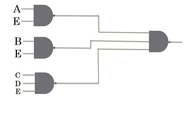
Method 2 (SOP Method):
The original circuit implements the Boolean function : (A+B+CD)E
We first manipulate this Boolean equation so that it is in the Sum of Products(SOP).
In this case, we simply multiply each term in the parenthesis by E.
We get: AE + BE + CDE.
Since this Boolean equation is now in SOP form, the circuit for this equation will be in a standard two-level implementation, meaning there will be a series of AND gates followed by a single OR gate.
We draw the circuit:
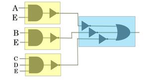
Just like in example 1, we insert two inverter gates between each AND gate and OR gate.
You can probably now figure out what we will do next. We combine the gates in the Yellow areas into one single NAND gate. Also, we know that an OR gate with complemented inputs implements a NAND operation. So we replace the gates in the blue area with a NAND gate.
Our final circuit:
We can conclude that whenever a circuit has a series of AND gates at the first level followed by a single OR gate, we can blindly replace each gate with a NAND gate and the circuit will still implement the same Boolean function.
In this case Method 2, took a lot less effort than Method 1, one might wonder why even bother learning Method 1 when Method 2 seems easier? The answer is that Method 2 requires that the Boolean equation must be represented in Sum of Products form. In this case, it was easy to convert our equation into SOP from, but this is not always the case.
Suppose you have a circuit that implements the Boolean function : (A+B)(C+D)(E+F)(G+H)
Converting this to SOP form will be complicated, and better with Method 1 in this case.
This article shows the effectiveness of the NAND gate in the field of digital logic design as explained before. This is desirable since by converting circuits to use only NAND gates, it is possible to simplify the designs for circuits, even if some penalties may be incurred in the process like the complexity of the gates. The NAND gate still continues to be significant because it is general-purpose.