 |
VOOZH | about |
|
VOOZH | about |
Latches are digital circuits that store a single bit of information and hold its value until it is updated by new input signals. They are used in digital systems as temporary storage elements to store binary information. Latches can be implemented using various digital logic gates, such as AND, OR, NOT, NAND, and NOR gates.
Latches are widely used in digital systems for various applications, including data storage, control circuits, and flip-flop circuits. They are often used in combination with other digital circuits to implement sequential circuits, such as state machines and memory elements.
Latches are basic storage elements that operate with signal levels (rather than signal transitions). Latches controlled by a clock transition are flip-flops. Latches are level-sensitive devices. Latches are useful for the design of the asynchronous sequential circuit. Latches are sequential circuit with two stable states. These are sensitive to the input voltage applied and does not depend on the clock pulse. Flip flops that do not use clock pulse are referred to as latch.
In digital electronics different types of latches are:
S-R latches i.e., Set-Reset latches are the simplest form of latches and are implemented using two inputs: S (Set) and R (Reset). The S input sets the output to 1, while the R input resets the output to 0. When both S and R inputs are at 1, the latch is said to be in an "undefined" state. They are also known as preset and clear states. The SR latch forms the basic building blocks of all other types of flip-flops.
The below table represents the truth table of SR latch.
S | R | Q | Q' |
|---|---|---|---|
0 | 0 | Latch | Latch |
0 | 1 | 0 | 1 |
1 | 0 | 1 | 0 |
1 | 1 | 0 | 0 |
SR Latch is a logic circuit with:
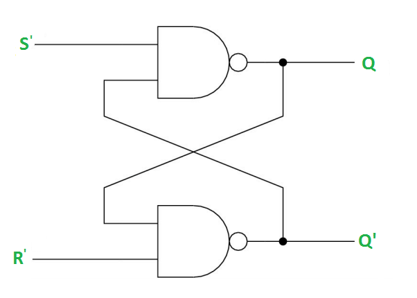
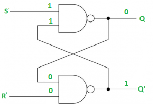
The below logic diagram represents the SR latch using NAND gate.
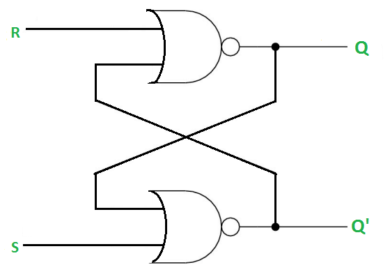
The below logic diagram represents SR latch using NOR Gate.
The different cases of SR latch are discussed below.
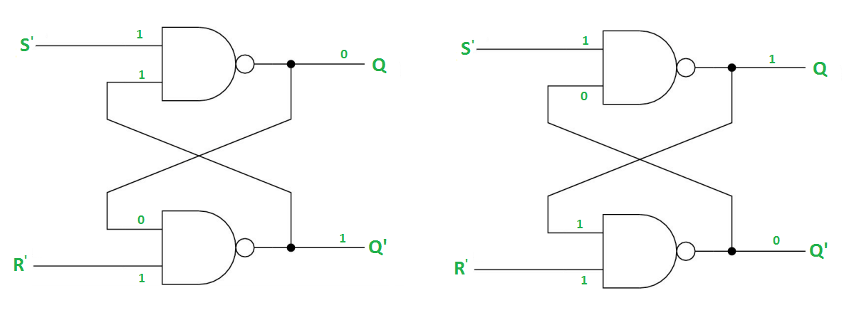
Case 1: S' = R' = 1 (S = R = 0)
If Q = 1, Q and R' inputs for 2nd NAND gate are both 1.
If Q = 0, Q and R' inputs for 2nd NAND gate are 0 and 1 respectively.
👁 Case 1: S' = R' = 1 (S = R = 0)
Case 2: S' = 0, R' = 1 (S = 1, R = 0)
👁 Case 2: S' = 0, R' = 1 (S = 1, R = 0)
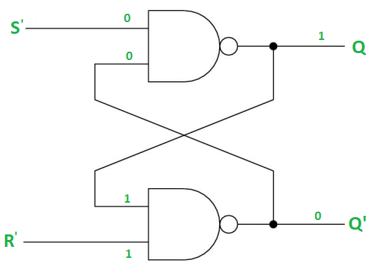
Case 3: S' = 1, R' = 0 (S = 0, R = 1)
👁 Case 3: S' = 1, R' = 0 (S = 0, R = 1)
Case 4: S' = R' = 0 (S = R = 1)
When S = R = 1, both Q and Q' becomes 1 which is not allowed. So, the input condition is prohibited.
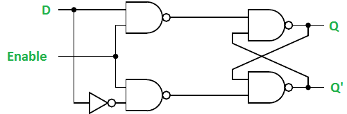
A Gated SR latch is a SR latch with enable input which works when enable is 1 and retain the previous state when enable is 0.
The below table represents the truth table of Gated SR latch.
Enable | S | R | Qn+1 |
|---|---|---|---|
0 | X | X | Qn |
1 | 0 | 0 | Qn |
1 | 0 | 1 | 0 |
1 | 1 | 0 | 1 |
1 | 1 | 1 | X |
The below logic diagram represents the gated SR latch.
D latches are also known as transparent latches and are implemented using two inputs: D (Data) and a clock signal. The output of the latch follows the input at the D terminal as long as the clock signal is high. When the clock signal goes low, the output of the latch is stored and held until the next rising edge of the clock.
The below table represents the truth table of D latch.
E | D | Q | Q' |
|---|---|---|---|
0 | 0 | Latch | Latch |
0 | 1 | Latch | Latch |
1 | 0 | 0 | 1 |
1 | 1 | 1 | 0 |
The below logic diagram represents the D latch.
D latch is similar to SR latch with some modifications made. Here, the inputs are complements of each other. The D latch stands for "data latch" as this latch stores single bit temporarily.
The below table represents the truth table of Gated D latch.
| Enable | D | Qn | Qn+1 | STATE |
|---|---|---|---|---|
| 1 | 0 | x | 0 | RESET |
| 1 | 1 | x | 1 | SET |
| 0 | x | x | Q(n) | No Change |
Characteristics Equation: Qn+1 = EN.D + EN'.Qn | ||||
The below logic diagram represents the gated D latch.
👁 Logic Diagram of Gated D Latch
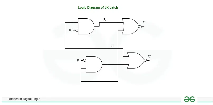
JK latch has two inputs J and K. The output gets toggled when the J and K inputs are high. JK latch is just like SR latch, but it eliminates the undefined state of SR latch.
The below table represents the truth table of JK latch.
J | K | Qn+1 | Comment |
|---|---|---|---|
0 | 0 | Q | No change |
0 | 1 | 0 | Reset |
1 | 0 | 1 | Set |
1 | 1 | Q' | Toggle |
The below logic diagram represents the JK latch.
When the JK inputs of JK latch are shorted we get the T latch. In T latch the outputs are toggled when the inputs are high.
The below logic diagram represents the T latch.
Some of the advantages of latches are listed below.
Some of the disadvantages of latches are listed below.
Here are a few books that you can refer to for further information on latches:
These books provide a comprehensive overview of digital logic, including latches, and cover various topics, such as design and implementation, simulation, and verification of digital circuits.
DIGITAL ELECTRONICS – Atul P. Godse, Mrs. Deepali A. Godse