 |
VOOZH | about |
|
VOOZH | about |
The NOT gate is one of the main building blocks of Digital Logic Circuits. A NOT Gate, also called an inverter, has only one input and one output. The output of the NOT gate is logic 0 when its input is logic 1 and the output is logic 1 when its input is logic 0. Thus, the output is always the complement of its input. Being a basic logic gate, the NOT gate is used in a variety of digital circuits to design and implement their basic logic circuits.
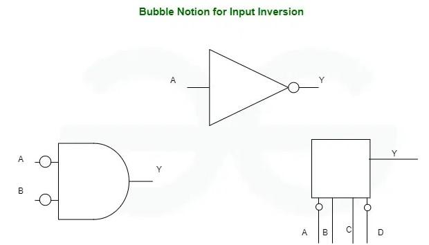
The logic circuit diagram of the NOT gate is shown in the following figure. It has only one input line denoted by the letter A and one output line denoted by the letter Y, where Y is the complement of the input signal applied to it. At the output line the bubble denotes the complement operation and it is called the inversion bubble.
NOT gate takes the Boolean value as input and returns the following results:
Returns 1, if the input is 0.
Returns 0, if the input is 1.
The Boolean expression of NOT Gate is as follows:
Y = Ā
or
Y = A'
Here the input variable to the NOT gate is represented by A and the output variable by Y. The symbol for NOT operation is ' - ' (bar) or ` ' ` (complement).
The truth table for the NOT gate is as follows. It shows the relationship between input applied and output generated and the working of the NOT gate for all the possible inputs. In a NOT gate, the output (NOT A) is the opposite of the input (A). So, when the input is 0, the output is 1, and when the input is 1, the output is 0.
In digital logic the Active-low Input Bubble is represented by a small circle at the input of a gate symbol which indicates that the logic level is inverted. In the case of a NOT gate, which performs inversion, the active-low input bubble indicates that the gates operation is inverted. So, when the input signal has the active-low bubble, it means that the gate will produce an output that is the inverse of the input signal.
Now we will see how we can form NOT gate using universal gates (NAND and NOR gate).
In digital electronics, we can implement the NOT gate logic by using the NAND gates only. For this, we tie all inputs of the NAND gate together and apply the input signal to the common input line as shown in the following figure.
The logical expression for this circuit is given by,
The NOR gate is another logic gate that can be used to implement the NOT gate logic. To realize the NOT gate circuit using NOR gate, we join all input lines of the NOR gate together and then apply the input signal to this common input line.
The operation of this circuit can be described using this equation,
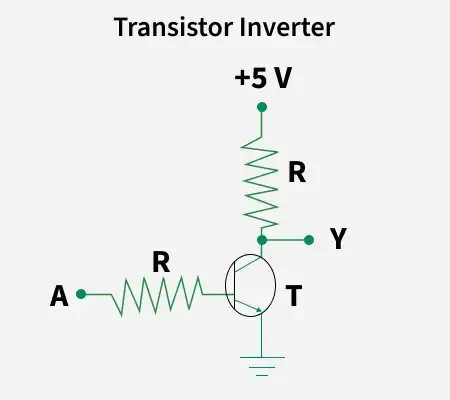
We can implement the NOT gate logic using a bipolar junction transistor. The circuit diagram of a NOT gate using BJT transistor is shown in the following figure.
A discrete NOT gate may be realized using a transistor as shown above. The input to the gate may be 0 V or +5 V. When A = 0 V, transistor T is reverse biased and, therefore, remains OFF. As no current flows through R, no voltage drop occurs across R. Hence the output voltage Y= +5 V. When the input A= +5 V, T is ON and the output voltage Y= Vcc (sat) ≈ 0V.
Truth Table for NOT Gate circuit:
A (Input) | Y (Output) |
|---|---|
0 V | 5 V |
5 V | 0 V |
There are some list of advantages and disadvantages of NOT Gate given below :
A person wants to design a robot such that it moves forward when the obstacle is not detected in front and it stops if there is any obstacle.
Solution: Let's build the truth table table:
The sensor sends ‘1’ when obstacle is detected and ‘0’ when obstacle is not detected.
Also, ‘1’ indicates the robot to move and ‘0’ to stop.
Obstacle Detection Sensor Output | Robot Movement |
|---|---|
0 (No Obstacle) | 1 (move) |
1 (Obstacle) | 0 (stop) |
To design a robot that moves forward only when there is no obstacle in front, we can use an obstacle detection sensor and a NOT Gate. The obstacle detection sensor will send '1' if the obstacle is present and '0' if it is absent. This output will be fed as input into the NOT gate, which will invert the signal. When an obstacle is not detected (A=0), the NOT gate inverts this to (Ā=1) , indicating that there is no obstacle, and the robot is allowed to move forward. When an obstacle is detected (A=1), the NOT gate inverts (Ā=0) indicating that there is an obstacle, and the robot is prevented from moving forward.
Design a street light mechanism in such a way that it is ON when it's dark and it is OFF during day.
Solution: Let's build the truth table table:
The sensor sends ‘1’ when it is detects light and ‘0’ when it does not detects light.
Also, ‘1’ indicates the street light to turn On and ‘0’ to turn Off.
Light Detection Sensor Output | Street Light |
|---|---|
0 (Light not detected) | 1 (On) |
1 (Light detected) | 0 (Off) |
To create a street light mechanism that is activated in darkness and deactivated during the day, we can use a light sensor and a NOT gate. The light sensor produces '0' when it is dark and '1' when it is bright. This output is then directed as input into the NOT gate, which inverts the signal. When it is dark (A=0), the NOT gate inverts this to (Ā=1), indicating that it is dark, and the street light must be switched On. Conversely, when it is bright (A=1), the NOT gate inverts (Ā=0), signifying that it is bright, and the street light must be Off.